

IMPORTANTI wanted to post this on GeekNews, but writing blog posts is a chore — so an AI ported my tidied-up project report into a blog post, and I finally sprinkled a bit of my own self on top. Just so you know.
If you sense both a human self and an AI’s tone in here, you’re exactly right.
How it started
Starting in the 2026 school year, under Article 20-5 of the Elementary and Secondary Education Act, smartphones can no longer be used at school.
The problem is that our school store’s payments run on DIMIPAY. You bring up a QR code in the app and scan it — without a phone, payment simply can’t happen. So we needed a way to prove identity without a phone, and that turned out to be the fingerprint.
To skip to the conclusion: I built it and deployed it at the store. Over the single month of May 2026, 3,199 of 7,454 total payments — about 43% — were made by fingerprint.
Demo video <- this right here is the hook.
There were quite a few constraints
For a hobby project you’d just hack it together and call it done, but this system handles real students’ biometric data. The requirements piled up in layers.
The kiosk is an iPad. Without MFi certification you can’t attach a wired accessory, which means communication has to go over BLE — the open API. Also, the sensor must not authenticate the user itself. It has to send the image to the server and let the server authenticate. The moment a fingerprint DB lives inside the sensor, it becomes unmanageable.
The legal side applies too. Under Article 21 of the Personal Information Protection Act, personal data must be destroyed once the purpose is fulfilled and the data is no longer needed; under Article 29, you must take technical, administrative, and physical measures such as establishing an internal management plan and retaining access logs. On top of that, the Personal Information Protection Commission’s biometric data protection guidelines require storing extracted minutiae rather than the original, and encrypting data in transit.
And authentication has to finish within 2 seconds
Picking a sensor
The requirements were these: if it uses USB, the protocol must be public; otherwise it must support an ordinary MCU interface like UART / I2C / SPI. And for authentication to succeed even with a high similarity threshold, the effective capture area has to be large.
After some searching I picked two.
| Product | Interface | Effective capture area | Role |
|---|---|---|---|
| HI-LINK ZW0608 | UART | 12.05×12.05mm² | For payment. Wired directly to the MCU |
| ZKTeco LIVE20R | USB 2.0 | 15.24×20.32mm² | For enrollment |
Honestly I wanted to do everything with the ZKTeco. The area is large and the images are good. But they don’t publish the USB protocol — they only ship Windows / Android / Linux SDKs.
So I captured USB packets with Wireshark and reverse-engineered the protocol, but stability was nowhere near good enough, so I scrapped it. In the end I put Android-based LineageOS on a Raspberry Pi to run the vendor SDK as-is, and decided to use that as an enrollment-only kiosk. Enrollment only happens once, so it’s allowed to be a bit slow.
The calculation was that if you build the template from a large image, even a small partial image would still produce a good matching score.
The matching algorithm
Proven reliability, template extraction support, and fast matching. With those three criteria in hand, I looked at two options.
NFIS
The one the FBI is known to use. It’s written in C, so it’s very fast, and it supports template storage.
But you have to build it yourself, and being legacy code it threw a mountain of build errors. There was too much code to fix by hand, so I gave up on that and barely managed to build and test it by recreating an old environment in Docker.
And then it was out. Its minimum supported image size was larger than the image the ZW0608 produces. It was unusable from the start.
SourceAFIS
You can approximately tune the FAR yourself by adjusting the score, templates are stored separately, and matching time is extremely short. It was ideal for the project I had in mind.
But the official implementations are only Java and .NET. Our backend runs on Bun.
I did consider porting it to JS, but raw computation is slower than on the JVM, and the time and effort the port would take were too great. So I settled for standing up one more Java web server, accessible only from the internal network. I built a server supporting fingerprint comparison/enrollment/deletion and deployed it internally.
Caching
It’s a bit embarrassing to call this an optimization, but fingerprint templates have to live in the DB, and you obviously can’t query the DB and compare everything on every lookup.
So at web server startup, I load all fingerprint data into memory — user IDs in one array, minutiae in another — and match against that cache.
The problem is when enrollment/deletion comes in at runtime. Get the ordering wrong and the cache runs ahead of the DB.
Enroll/delete request
      │
      ▼
  Run DB transaction
      │
      ▼
  Commit succeeded?
   │      │
  Yes     No
   │      │
   ▼      ▼
Lock cache,   Rollback
apply change  cache untouched
Cache updates only ever happen after the DB commit.
V1 hardware
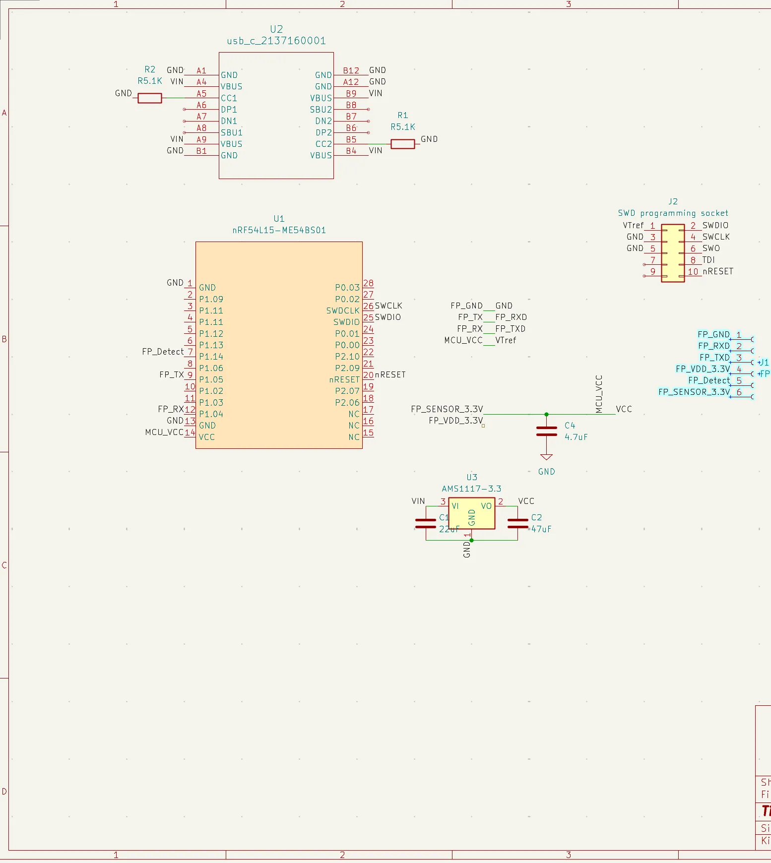
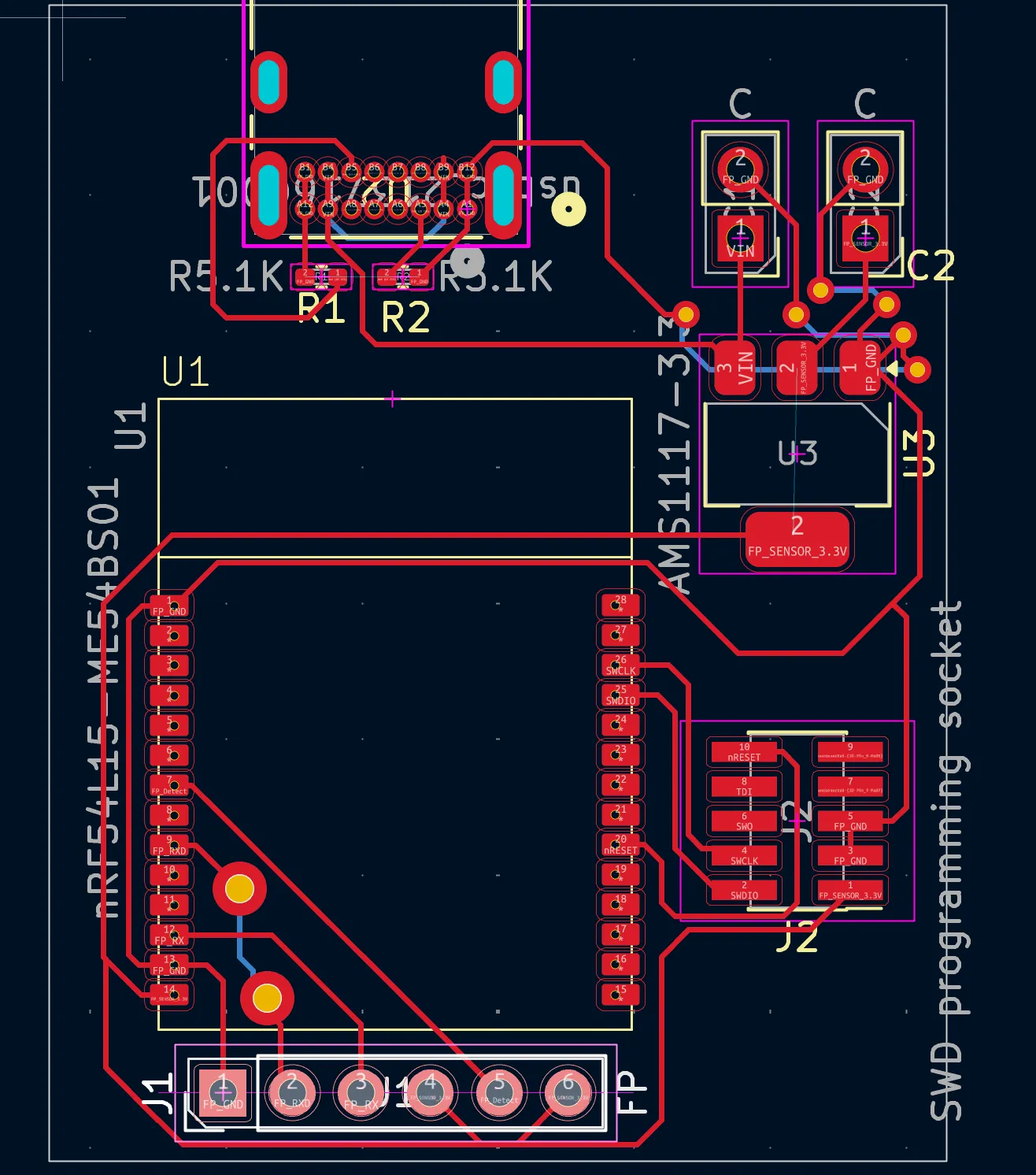
Since BLE was mandatory, I figured a BLE-integrated MCU was the right call, and picked the nRF54L15 — which I happened to be learning at the time.
But there was no time to design a board from scratch. The start of my third-year first semester was less than two weeks away, and the school intranet development deadline was the top priority. So I designed around MINEWSEMI’s nRF54L15-ME54BS01 module. The module takes care of the RF side.
SourceAFIS ──Internal HTTP── Core Backend
                                  │
                                HTTPS
                                  │
                                iPad
                                  │
                           BLE (encrypted)
                                  │
                             nRF54L15 ──UART── ZW-0608
The flow goes like this. The nRF54L15 subscribes to the ZW-0608’s finger interrupt line, and when the interrupt fires it notifies the iPad kiosk app. If the kiosk happens to be at the payment step, it calls the controller’s fingerprint-payment function. An image transfer request then goes down, the MCU issues a capture to the ZW-0608, and pulls the image out of the sensor buffer over UART. That’s handed back to the iPad over BLE, the iPad fires it off to the server, and the server verifies the identity.
Clean. And it worked. The problem was speed.
And then, 5.8 seconds
Average authentication time came out at 5.8 seconds. The requirement was 2 seconds.
I broke the time down in detail.
├────────── 3.8s ──────────┼── 1.0s ──┼─ 0.7s ─┼0.3s┤
      Sensor → MCU           MCU→iPad   server   other
         (UART)               (BLE)    round trip
                  ┊
             requirement 2.0s
The single UART upload segment was eating roughly two-thirds of the total time.
Even squeezing the transfer stage as hard as possible with compression or whatever else, the UART baud rate ceiling means you can’t get below 3.8 seconds. This isn’t a problem optimization can solve — the interface choice was simply wrong.
If speed were the only problem that’d be one thing, but accuracy was iffy too. Thanks to the Live20R’s large images I got the average matching score up to around 50, but fingerprint quality varies so much between people that uniform accuracy was hard to guarantee. If recognition fails on the first try you have to retry — and one try is 5.8 seconds. At a store during lunch and dinner peak hours, where fast turnover is essential, it’s simply unusable. The line backs up.
The PCB had problems as a bonus. I ordered it with UART RX and TX mapped backwards. Fixed by swapping the wires. Also, on a 2-layer board with no GND pour on the back layer, I never tied the GND of the LDO power block that converts VBUS 5V to VDD 3.3V. That happened because I just dropped in a GND via without any GND pour… Fixed by bridging it with hand soldering.
Looking back
I had a lot of thoughts.
Originally I finished testing with the ZW-0901 on the DK and rushed the PCB order, but partway through testing the recognition rate dropped on other people’s fingerprints, so I hastily switched from the ZW-0901 to the ZW-0608. As a result there was no time to properly test the transfer speed. I could have estimated it from the data volume, but I was in the middle of troubleshooting and patched things up in a hurry without weighing everything. It was a shame that this blew up exactly as you’d expect.
The PCB was a disaster too. The IFA antenna needs a keep-out area and I didn’t respect it, and a 3.3V power line ran right underneath the antenna. Worse, I had originally planned to hand-fabricate it, so the via sizes I’d chosen for that carried straight over into the fab order, making the vias abnormally large, and there were plenty of sharply bent traces. It was lucky there were no impedance-sensitive high-speed lines — it was not a good design.
Truly nothing about the design was right, but as a silver lining(?), forgetting the GND pour meant RF performance was never wrecked. Had there been GND under the antenna, that would have been the bigger problem.
I’m left with the regret that if I’d given myself just a bit more breathing room, I could have turned out a far more polished prototype.
So for V2 I started over from the sensor. Continued in the next post.