

In the previous post I talked about how V1 got stuck at 5.8 seconds because of UART. This time it’s about tearing that down.
One more line added to the requirements
Exactly one line was appended to the V1 requirements.
A fingerprint sensor supporting SPI communication at 12MHz or above
Never again am I using a 3.8-second UART.
Sourcing a sensor
Having confirmed that off-the-shelf fingerprint sensors have clear limits, I started contacting manufacturers directly.
| Manufacturer / model | Interface | Image | Verdict |
|---|---|---|---|
| CAMABIO | UART, USB (protocol undisclosed) | - | The sensor itself was ideal, but out due to no SPI support + undisclosed USB protocol |
| Midas Touch MFC-1208GD | - | Fewer pixels than the HF302GD | Out due to insufficient pixel count |
| Aratek A400-M | - | - | Operating voltage doesn’t match the MCU. Out because it would need extra level-shifting design |
| ADH-TECH HF302GD | SPI 16MHz | 256×360, 508dpi, up to 9fps | Selected |
In the end I went with ADH-TECH’s HF302GD. It can deliver images over SPI at 16MHz, and 256×360 at 508dpi gives plenty of both area and resolution. Capture is fast too, up to 9fps.
POC
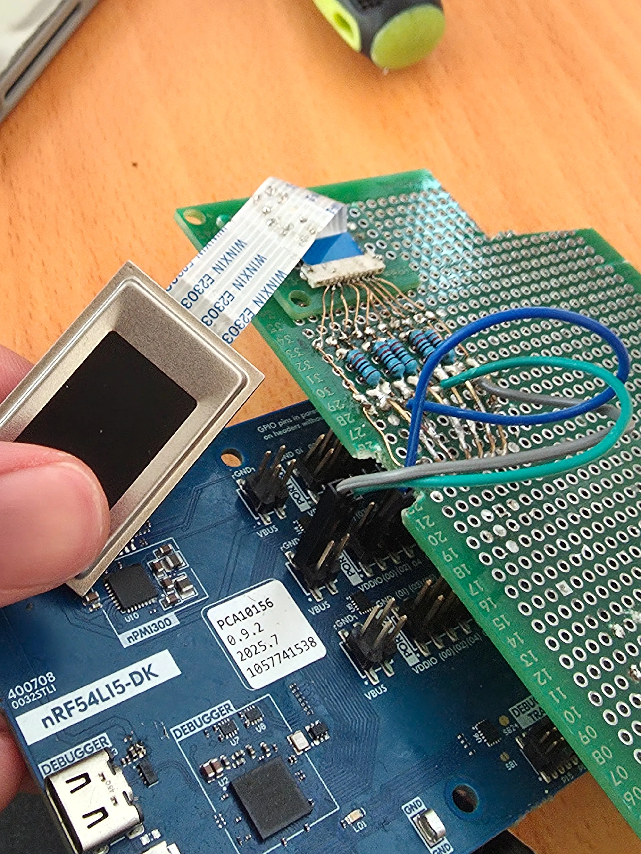
I contacted ADH-TECH by email and bought a hardware sample and a test board.
The moment it arrived I pulled the FPC connector off the test board, soldered it to perfboard, wired up power and the SPI data lines, and hooked it to the nRF54L15-DK. That’s the hardware POC. With operation confirmed, it was time to design the board.
Board design
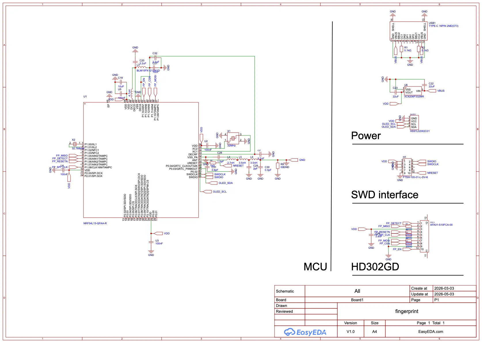
This time I had enough time and budget, so I decided to design a board with the nRF54L15 mounted directly and have it assembled (PCBA). I normally use KiCad, but drawing it in EasyEDA came with an ordering discount, so I switched. Unlike KiCad, you can search the JLCPCB Components Lib and drop parts straight in, and not having to write a separate BOM was definitely convenient.
I designed it with reference to the Reference Circuitry in Nordic’s nRF54L15 datasheet, and for the power section, filters, and RF circuit I adopted the datasheet’s BOM spec verbatim to guarantee reliable operation. There’s no reason to get creative here.
To keep the 2.4GHz antenna simple, I copied the IFA straight into the circuit from TI’s AN043 Application Note, then had the design verified through Nordic Q&A. On the SPI lines between the fingerprint sensor and the MCU I added the 200Ω ringing-suppression resistors specified in the sensor manufacturer’s datasheet.
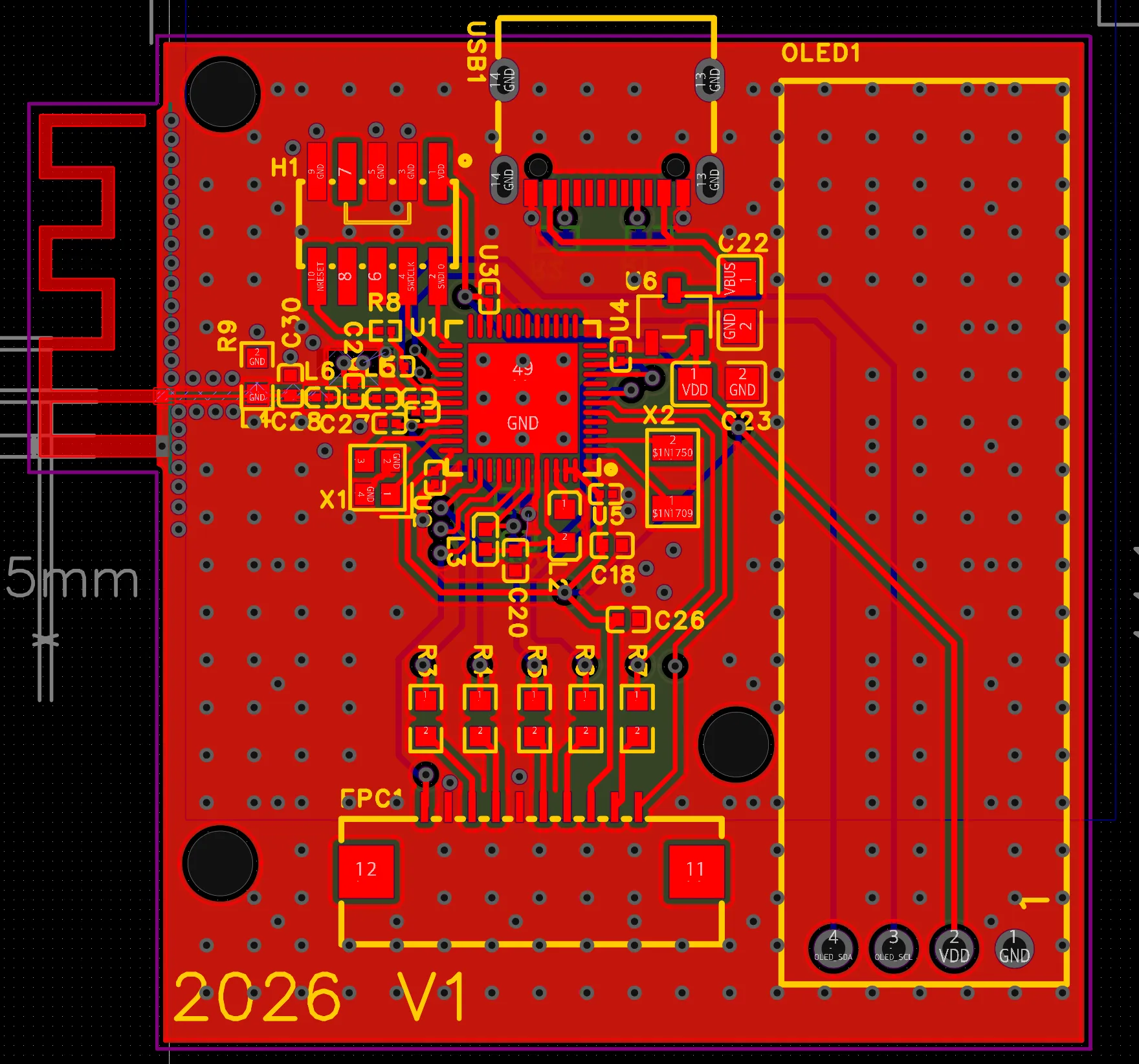
I also added an OLED.
The dev team can’t attach via SWD every time just to read the BLE passkey and pair, nor can they camp at the store managing the device. So I added an OLED module, letting the store staff handle pairing, status checks, troubleshooting, and even error reports for the dev team just by looking at the board.
Power comes in through the USB-C at the top of the board. With 5.1k on the CC pins, it takes 5V into VBUS per the USB 2.0 spec, and an LDO steps that down to 3.3V for VDD. Bulk capacitors before and after the LDO create a buffer on the common power rail.
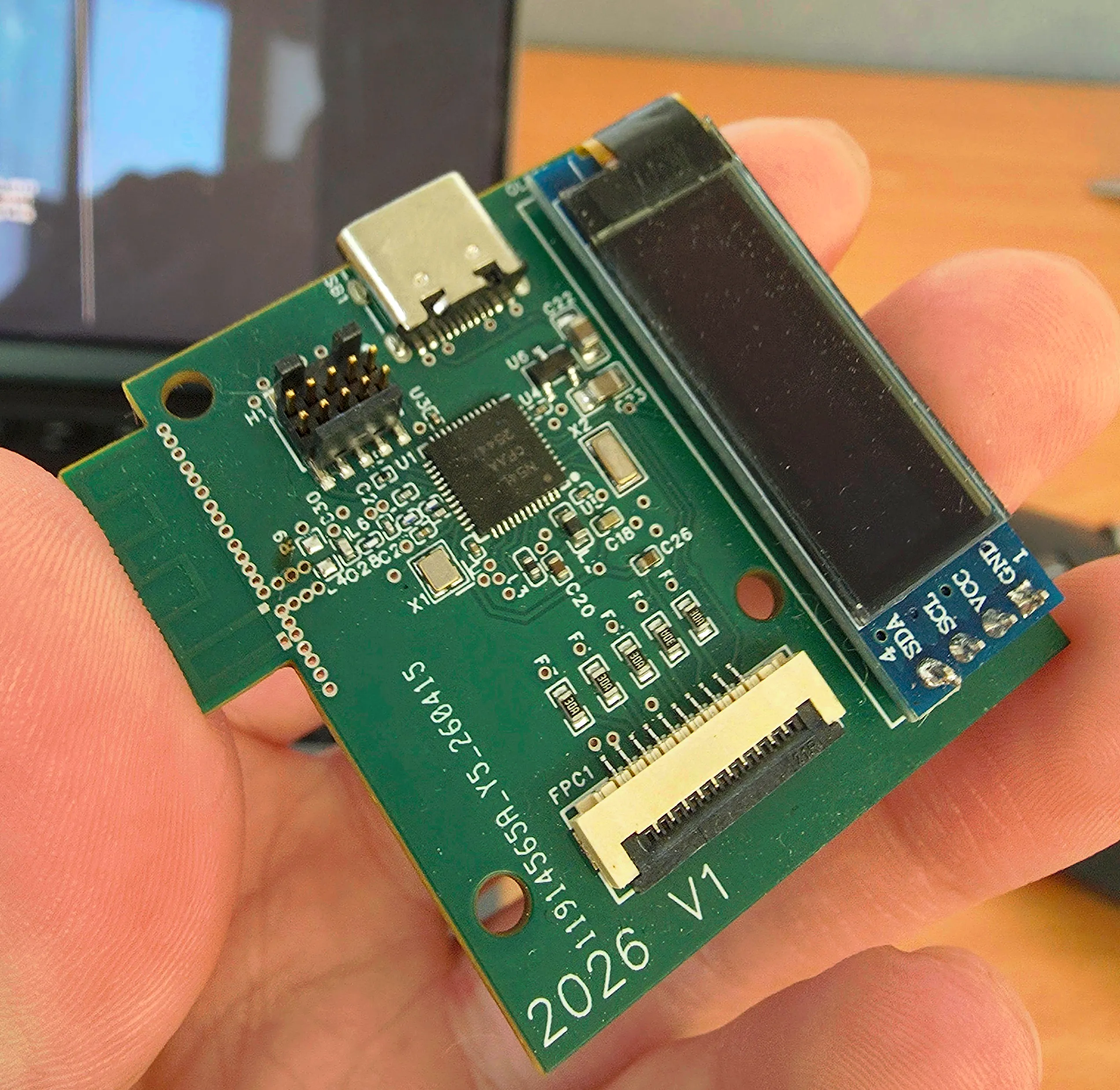
This is the assembled board as received.
I split the vias by purpose too. Suture vias tying the ground and power planes together have no exposed via pad, while vias on decoupling and data lines expose their pads so they can double as test points. That is exactly what saves my life in the next chapter.
Failed to power up DAP
I got the board, connected power, and tried to attach to the DAP:
TF9FD58C0 005:626.736 Found SW-DP with ID 0x6BA02477
TF9FD58C0 005:628.365 Failed to power up DAP
TF9FD58C0 005:680.817 ConfigTargetSettings() start
TF9FD58C0 005:681.040 InitTarget() start
TF9FD58C0 005:682.630 InitTarget() end - Took 1.53ms
TF9FD58C0 005:788.991 Failed to attach to CPU. Trying connect under reset.
TF9FD58C0 005:790.139 Found SW-DP with ID 0x6BA02477
TF9FD58C0 005:790.720 SWD speed too high. Reduced from 4000 kHz to 2700 kHz for stability
TF9FD58C0 005:791.796 Failed to power up DAP
TF9FD58C0 005:791.837 - 169.767ms returns 0xFFFFFEFB
It finds SW-DP but can’t power up. And the returned values looked random — meaning it can’t return proper results. I judged that the DAP itself was unable to respond.
The prime suspect is obviously power
Since the error says “power,” power was the first thing I suspected.
Looking into it, I had indeed forgotten to connect the 3.3V rail to the 100nF decoupling cap mapped to pin 10. “Ah, this is it,” I thought — but probing with a scope showed the voltage was stable, and connecting it changed nothing.
That wasn’t the cause.
DECA is oscillating
While continuing to debug by moving the probe around (those test points I made earlier really shone here), I found it.
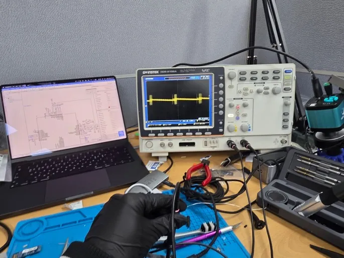
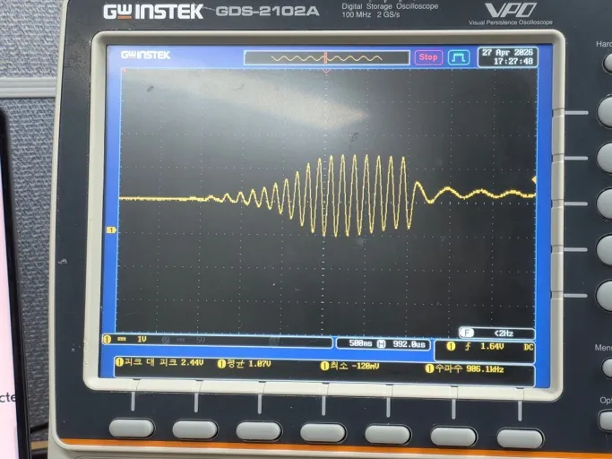
The DECA line was oscillating at 8MHz.
I then started tracking down the cause, resoldering various components,
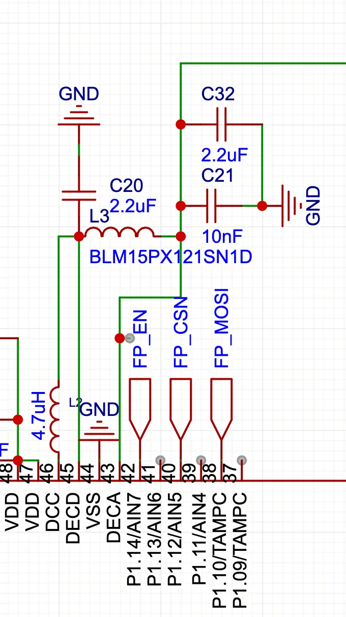
and found that removing C21 in the circuit above made the oscillation disappear. C32 is a component added after root-causing and fixing the issue, to eliminate the problem in production. It isn’t on the actual PCB.
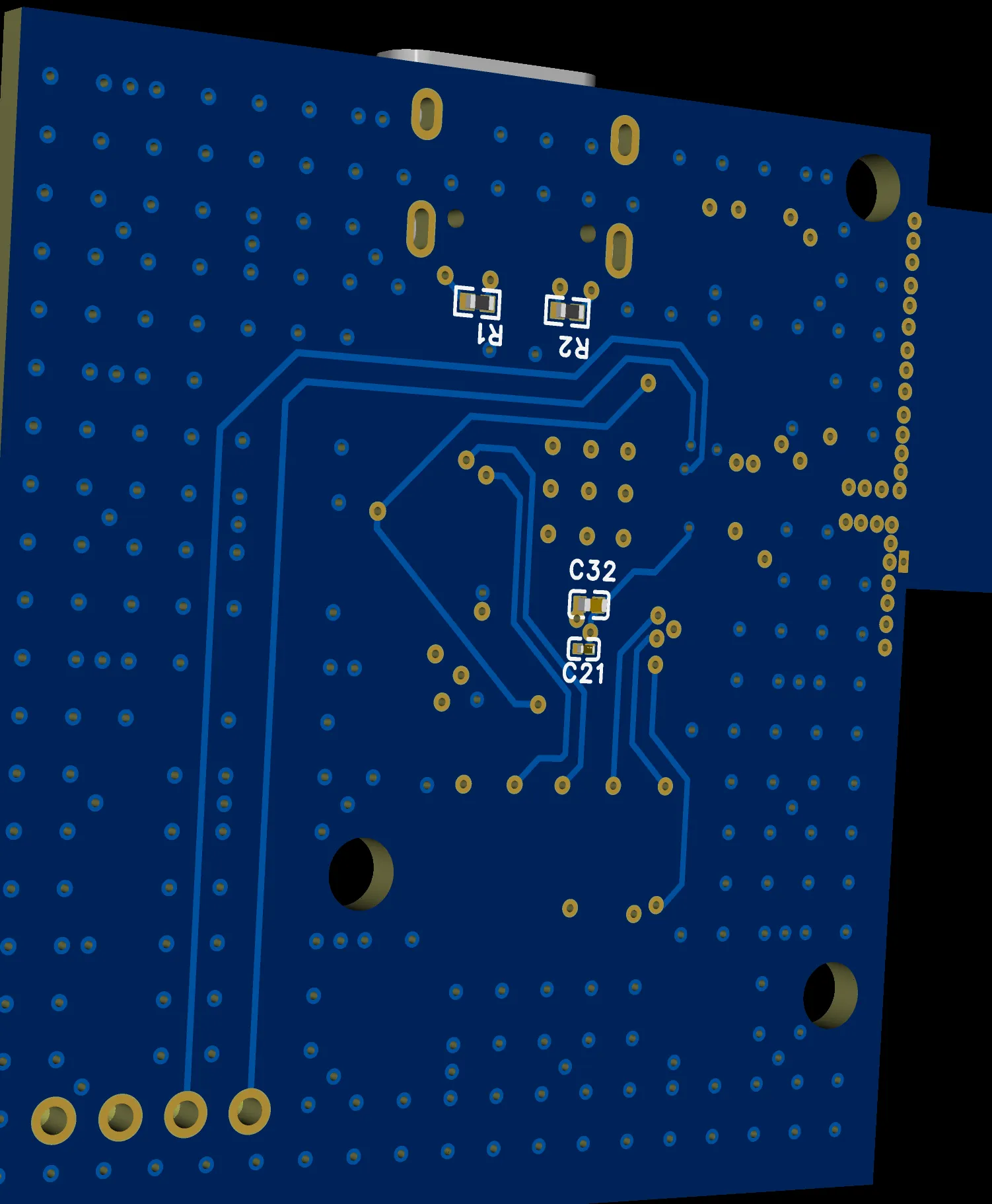
It’s that 10nF sitting awkwardly on the back of the board.
First hypothesis,
Here’s what I thought at this point.
At 8MHz it’s hard to call it LC resonance. I figured it was more likely the buck converter output being very slightly smoothed by C21.
The nRF54L15 has both an LDO and a buck converter in its internal power stage. At startup it draws power through the LDO while detecting whether an LC circuit is present at the buck converter output, and if nothing is detected it keeps running on the LDO. But this inductor-detection circuit doesn’t really look at the inductor itself — it’s closer to detecting the oscillation an LC circuit produces. So did that awkwardly placed 10nF on the back of the board put it into a “detected” state, causing the buck converter to run and oscillate at that frequency?
So I compared the reference circuitry against mine line by line, confirmed that the 2.2uF (C31) was missing, and the problem was solved once I added it. My question on Nordic DevZone also got the reply that C31 was missing, so the circuit itself was confirmed.
But revisiting this after the fix, I realized my reasoning had been flawed.
Looking again at the regulator diagram, the buck converter switch output is the DCC pin, and a capacitor and inductor are already connected there. DECA, meanwhile, is a line tied directly to the LDO. In other words, seeing oscillation on DECA means the problem was in startup or in analog peripheral initialization — not the buck converter.
I ruled out the RF side too. During root-causing, when I cut the DECRF connection trace and tested, the DECRF line was stable and only DECA remained unstable.
And here the logic tangles. If failed power stabilization were the cause, then removing the 10nF (C21) should, if anything, make it stop working. But removing it stopped the oscillation. Why?
The answer came much later
I left it as an open question and moved on to other projects, until one day I suddenly wondered “why does an LDO need a decoupling capacitor at all?” and dug in a little.
Until then I’d thought of an LDO as just a passive component. A box where you put in 5V and 3.3V comes out. So I’d never questioned it.
But that was wrong. An LDO uses a feedback loop to modulate an internal P-MOS gate, producing a resistance, and creates the target voltage from that divider. It’s an active device. Once I understood that, the identity of the output capacitor became clear too: it exists to suppress voltage rise/fall during the window when the resistance is still changing — before the LDO’s feedback loop catches up with an increase or decrease in load.
At that point the 8MHz was explained. 10nF is far too small to absorb the variation in that window. So the change in output voltage and the change in resistance driven by the feedback loop kept inverting against each other, producing oscillation — a phenomenon that showed up precisely because the 2.2uF that would have damped it was missing.
Removing just C21 stopping the oscillation has the same explanation: a component participating in the oscillation loop disappeared. The right answer was not to remove C21 but to add C31, and that is how it was ultimately fixed.
If there’s a lesson, it’s that the reference circuitry’s BOM exists to be followed exactly. Drop a single capacitor and SWD won’t attach. What a pain
The next post covers the firmware and fingerprint binarization.