

IMPORTANTNote: this post is my own reconstruction of what I understood after watching videos by Ben Eater and Core Dumped.
tl;dr
| N-type semiconductor | P-type semiconductor | |
|---|---|---|
| Element | Phosphorus | Boron |
| Charge | Negative | Positive |
| Carrier | Free electrons drift | Electrons hop into holes |
- Join the two semiconductors and connect the negative terminal to the N side and the positive terminal to the P side: the PN junction thins out and eventually collapses, electrons move from N toward P, and current flows.
- Wire it the other way around and the depletion region of the PN junction widens, so electrons don’t move and no current flows.
Introduction
Through doping, semiconductors split into two kinds: P-type and N-type.
Which one you get basically depends on which element is added to a silicon-based material.
N-type semiconductor
An N-type semiconductor is a silicon-based material that contains phosphorus.
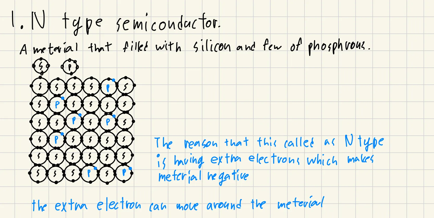
In a silicon-based material the atoms covalently bond to each other, leaving almost no free electrons, so the material behaves like an insulator. But by mixing in phosphorus, which has five valence electrons, surplus electrons are created, and those surplus electrons can roam freely through the material. That gives the material — the N-type semiconductor — its conductivity.
NOTEIt’s called N-type because the extra electrons give it a negative charge.
P-type semiconductor
A P-type semiconductor is a silicon-based material that contains boron.
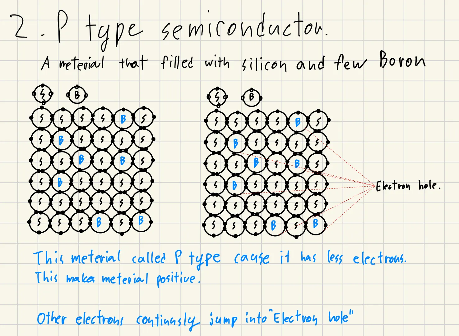
Just as with the N-type, a silicon-based material covalently bonds with itself, leaving almost no free electrons, so it behaves like an insulator. But by mixing in boron, which has three valence electrons, holes are created; another electron fills a hole, and yet another electron moves into the new hole that is left behind. In this way the material — the P-type semiconductor — gains its conductivity.
NOTEIt’s called P-type because having fewer electrons gives it a positive charge.
Putting it to use (the diode)
With P-type and N-type semiconductors you can build a diode, which lets current flow in only one direction.
How? Just stick them together!
PN Diode
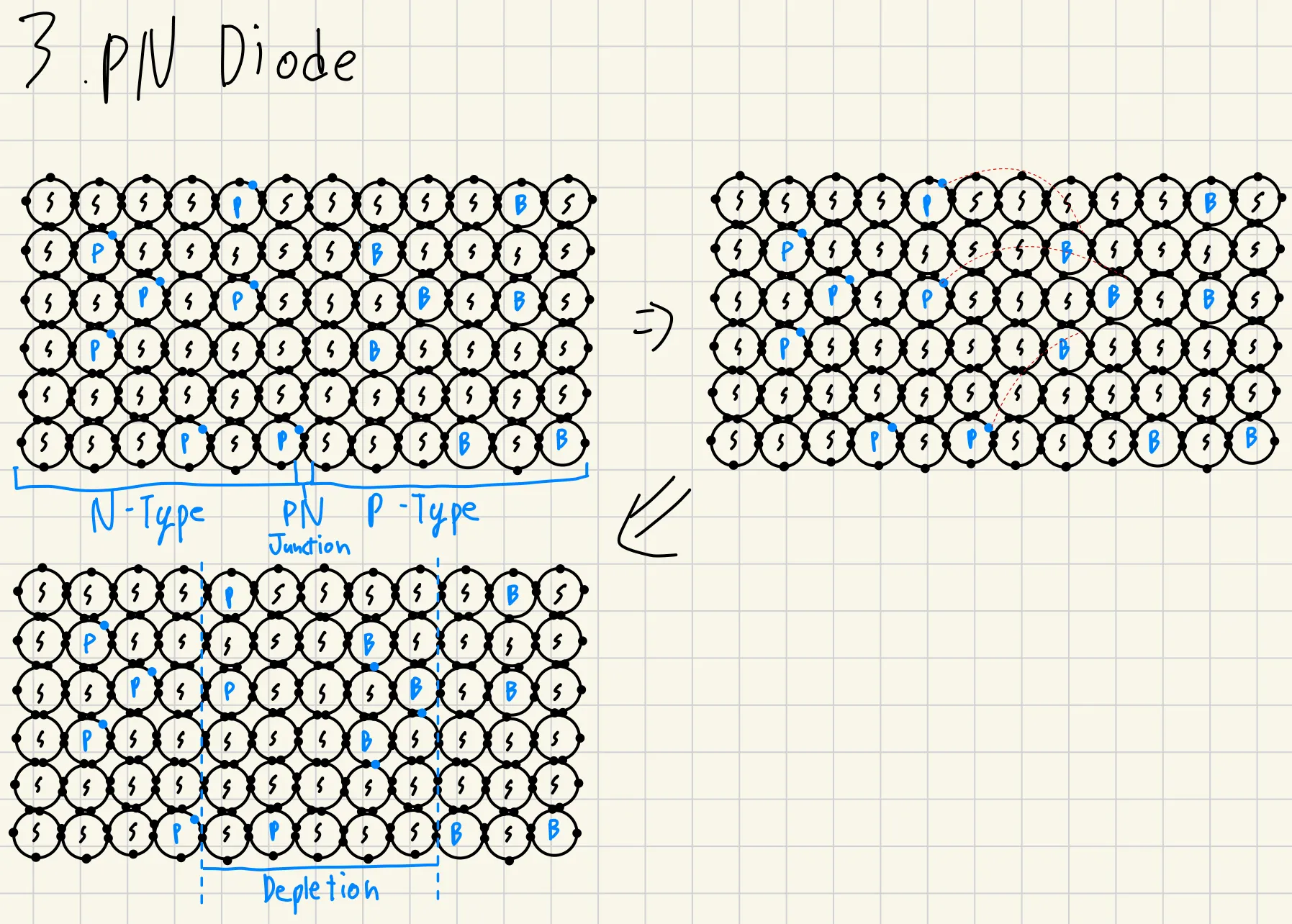
When you join the two semiconductors, free electrons from the N-type move into the holes of the P-type! As a result, a depletion region forms around the PN junction (the boundary), creating a stable middle zone.
What if we connect a battery? (positive terminal to the P-type)
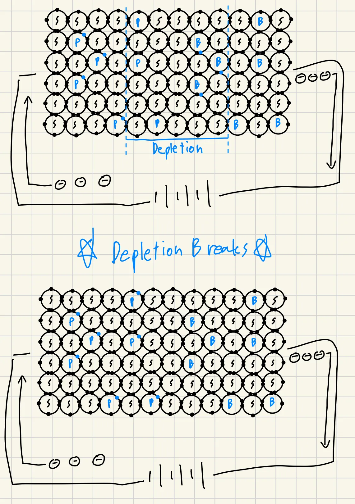
Electrons move into the N-type and free electrons fill the depletion region, while electrons on the P-type side move into the battery, creating holes. As a result the depletion region shrinks as the voltage rises. And the moment the voltage reaches a certain point, the depletion region collapses and current flows.
What if we connect a battery? (positive terminal to the N-type)
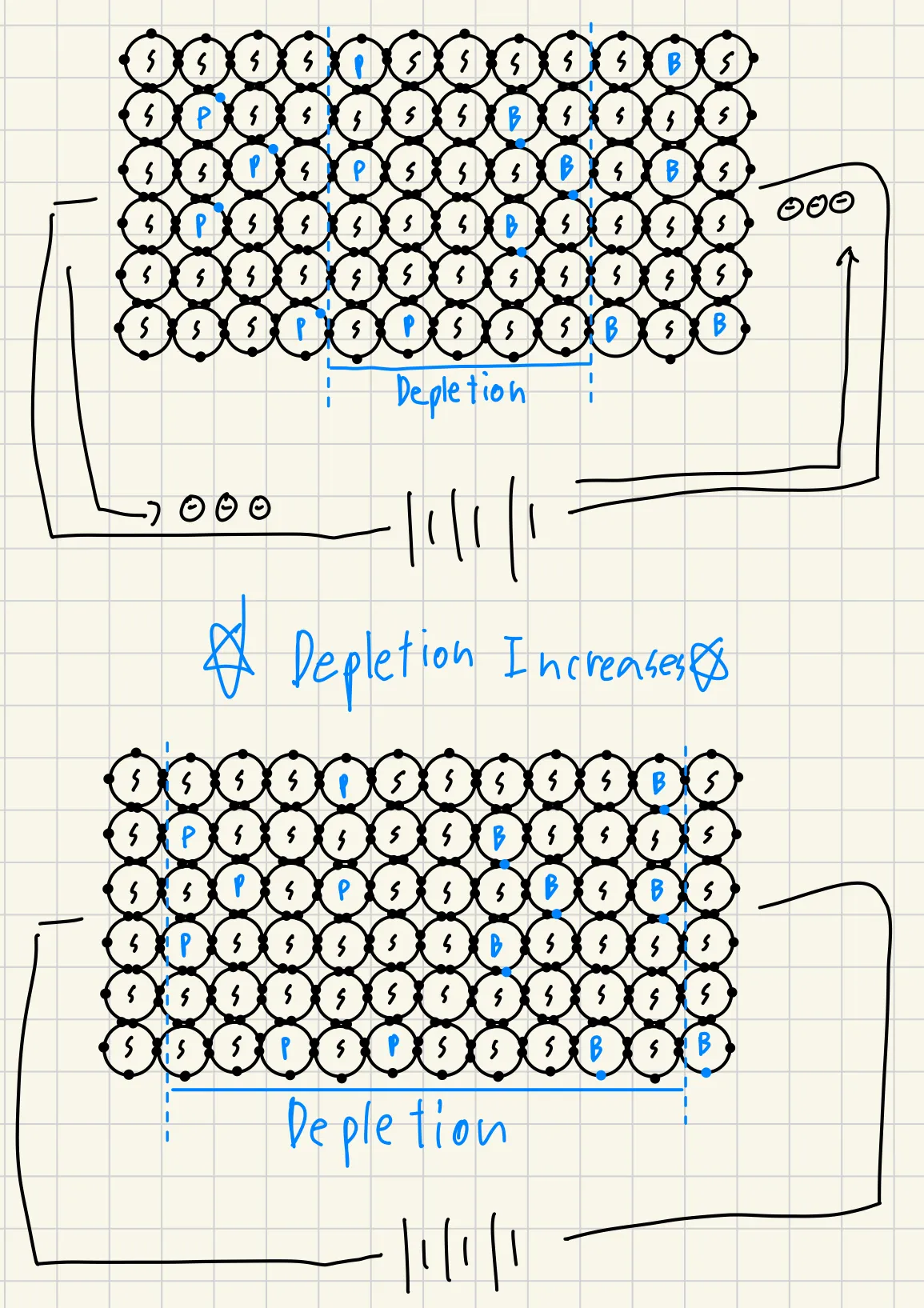
Free electrons in the N-type move into the battery, and free electrons fill the holes in the P-type, so the depletion region widens. In other words, in this configuration no current flows no matter how hard you try to push it.