
TIP
The need for a reliable, highly integrated stepper driver
Though can a stepper driver I built myself really be called reliable
Anyway, setting that aside — I’d bought nine TB6600s and was using them! But maybe because I bought them from a sketchy seller, they kept dying one by one! SHIT!
So my stepper driver count kept shrinking, and on top of that the TB6600 was extremely inconvenient and annoying to power and wire up to a Nucleo-F446RE.
So I thought, if it’s going to be like this, let’s just build one! — and started designing.
The reason I built it myself rather than buying another commercial product is that with each project my circuit design skills visibly accumulate, and that itself is motivating.
The initial requirements were roughly these.
- Per-channel current limiting, since the motors I use are all different
- Tolerate around 36V (typical for Saehan Electronics steppers) to secure high-speed torque
- An I2C interface to take encoder input
Main configuration
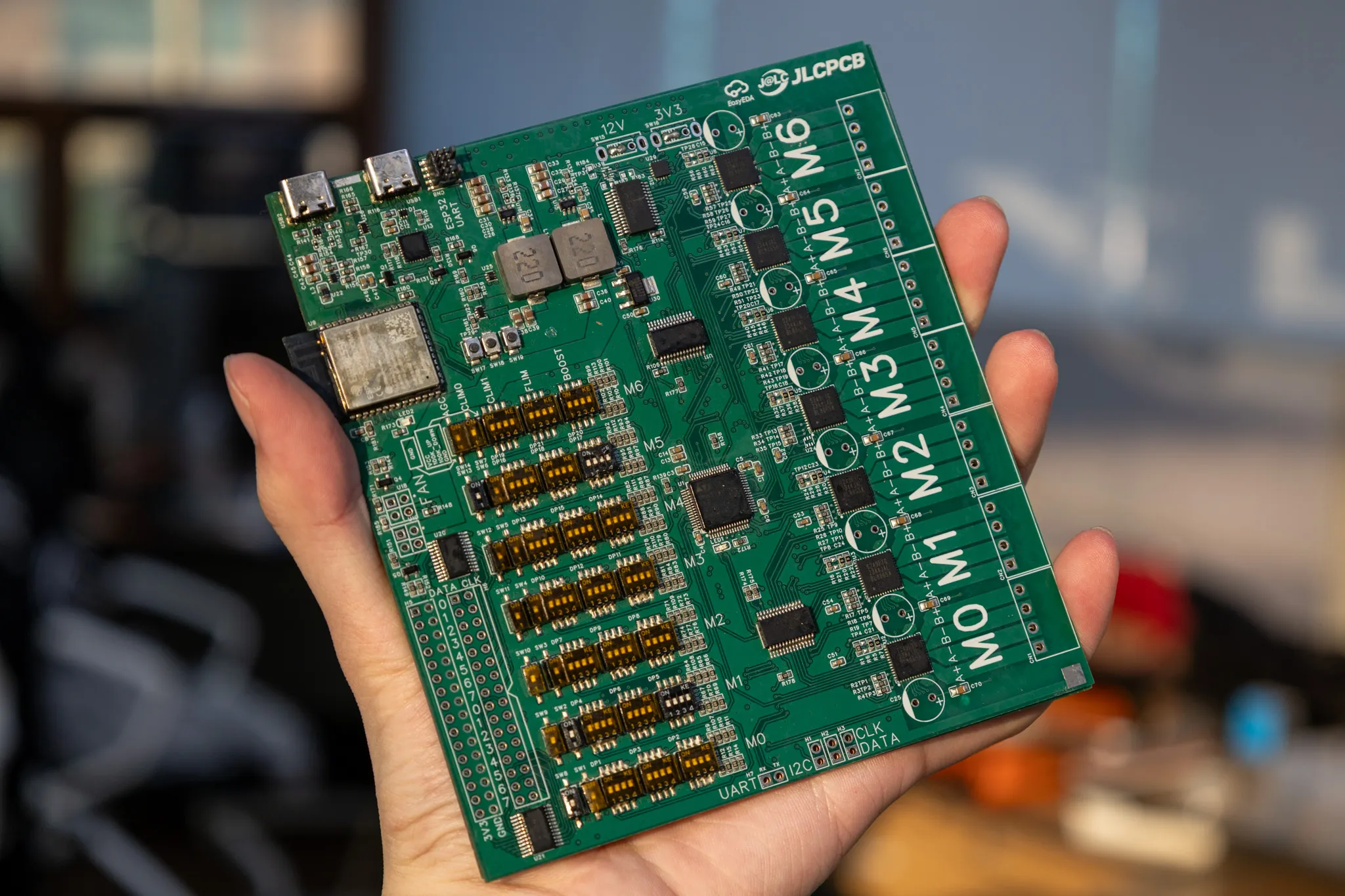
Not an AI…
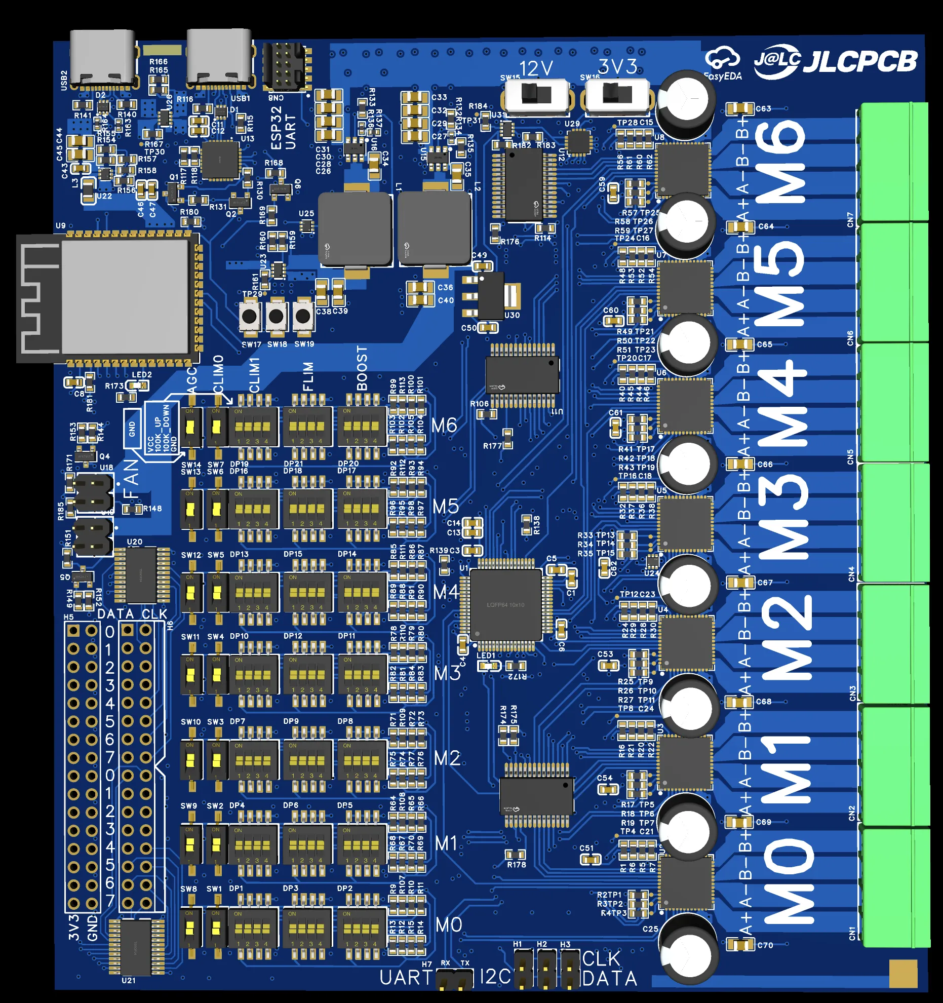
- Dimension: 121 x 132 mm^2
- STM32F446RE Low level driver
- ESP32-S3 Communication / IK Solver
- x7 TB67S249FTG Step Controller
- x2 TCA9548A I2C Mux
- x2 PWM Fan Interface
The power range set during design is as follows.
- Voltage: 12V ~ 46V
- Maximum current: 35A (driver) + 3A (peripheral) = 38A
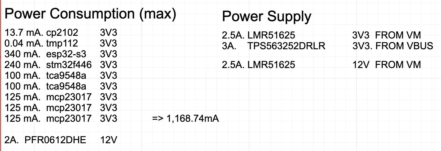
The peripheral side draws 1.168A / 3.8544W on the 3V3 domain and up to 2A / 24W on the 12V domain, about 28W total. Converted to a 12V basis that’s about 2.3A, but since I might add more I2C sensors later I left headroom and set it at 3A. (Peripheral current draw can vary with input voltage.)
A dual-domain control section
This board uses the STM32F446 as a dedicated motor-control controller, and the ESP32-S3 as the processor that interfaces with external devices, receives commands, and solves IK.
External host ──USB/Wi-Fi── ESP32-S3 ──SPI+UART── STM32F446 ──CLK/DIR/EN── drivers x7
               (processor)             (controller)
I split them to separate the domain that focuses purely on low-level motor control, receiving target angles or speeds in real time and executing them, from the domain where latency can creep in — networking, USB, inverse kinematics. But why did I not think about I2C latency at this stage…
The two chips communicate over SPI. This line is used when the processor reads status values or hands sequenced joint targets to the controller.
I also wired the processor so it could drive the controller’s STM_NRESET_FROM_ESP and BOOT0 directly, intending to manage the whole controller remotely — but I mixed up which of SPI2’s two wirings the bootloader uses, so firmware updates ended up being SWD-only. A shame.
Power: using motor power and USB power together
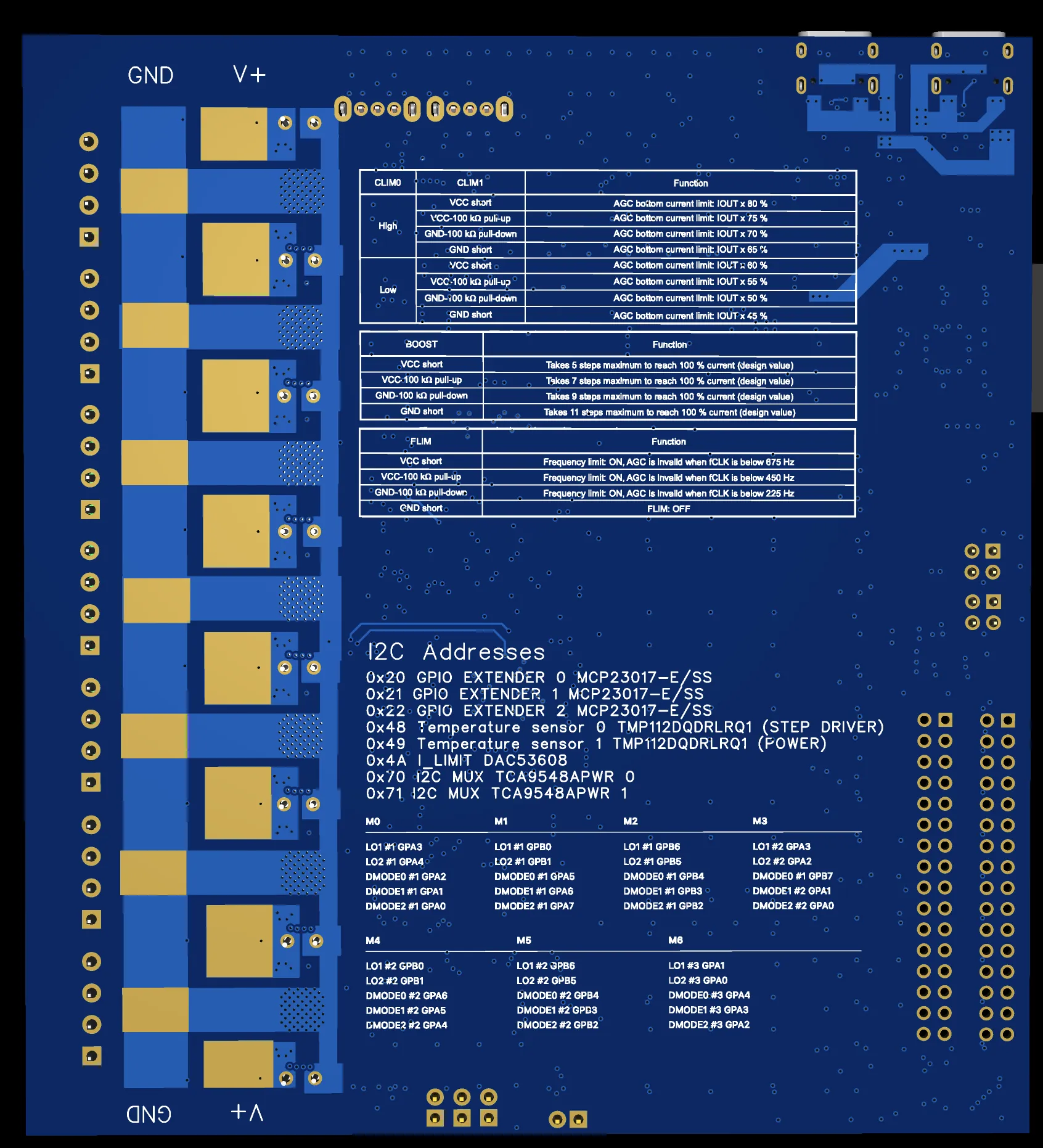
Power comes in via a copper busbar soldered to a surface-finished copper plane exposed by stripping the solder mask on the back of the board.
Up to 40A has to flow, and handling that with in-board copper alone would require widening or thickening the copper, which sharply raises manufacturing cost. So I routed the main current through an external busbar. To get past DRC I did tie the nets internally and laid down a plane wider than the signal traces, but that isn’t the main current path.
This power feeds the stepper drivers directly and branches off into the other power domains from there. The Vmotor copper is laid on three layers — top, inner2, and bottom — and arranged to flow in only one direction, from the right side where the seven drivers sit toward the left where the logic is, so that the motor current’s return path never crosses the logic area.
Voltage tree
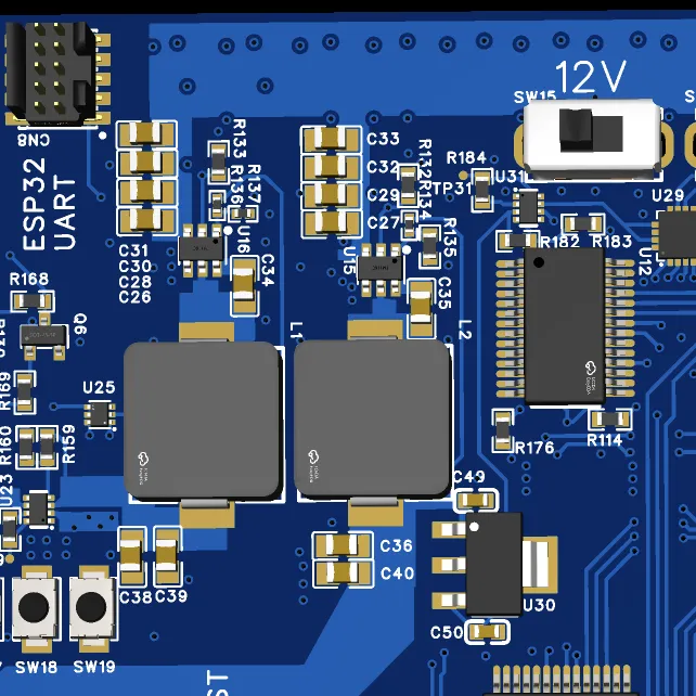
The main bus splits in two and steps down to 3V3 and 12V through an LMR51625 each. I chose the LMR51625 because its 65V input rating leaves headroom over the 46V design ceiling, and because it can drop from Vmotor to logic voltage in a single stage.
3V3 is the logic-level rail running things like the MCUs, while 12V either drives the fans directly or passes through an LDO to the DAC, where it’s used to generate the current-limit reference voltage.
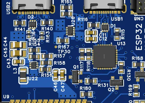
Without main power, it can take 5V from USB and generate logic 3V3 and DAC 5V through a TPS563252. VBUS from USB2, which attaches to the ESP32-S3’s USB PHY, takes priority; failing that, USB1’s VBUS is used. A TPS2116 power mux picks between them.
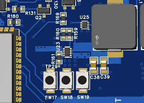
Likewise, between the 3V3 generated from the 5V domain and the 3V3 generated from the Vmotor domain, a power mux selects the Vmotor side by preference. Thanks to putting a power mux on each domain, USB can be plugged in safely even while Vmotor is present.
In summary:
V_motor 12~46V (bus bar) ── LMR51625 U16 ──┐
                                           ├─ TPS2116 U23 ── 3V3 (logic)
USB1/USB2 VBUS ── TPS2116 U26 (5V) ── TPS563252 U22 ──┘
                          │
V_motor (busbar branch) ── LMR51625 U15 ── 12V ── fans x2
                                          │     5V
                                          └─ MCP1799 + TPS2116 (5V_DAC) ── DAC53608 V_REF x7
I took only the DAC rail from an LDO rather than a switcher because I thought one more buck converter would noticeably inflate the BOM. But thinking it over, JLCPCB charges a $3 setup fee for each extended part added, and the TPS563252 already used for 5V→3V3 is small and already in use — so no setup fee, and only $0.3 extra. Meanwhile the LDO was $1.2 apiece. It was a completely wrong call…
Well, it’s water under the bridge, and since the TB67S249FTG’s current-limit input pins are hi-Z and draw almost no current, the current on the DAC input side is effectively nil. So the LDO is in fact sufficient.
Driver selection
I used seven TB67S249FTG drivers. Why I picked it:
- No external FETs required
- High current capability
- Simple dir/step driving, with no complicated I2C or SPI setup
- Microstepping support
- AGC support
This project uses two stepper types, NEMA17 and NEMA24, and the NEMA17 runs far hotter at rated current than expected — which made the AGC feature listed in the datasheet’s features section look extremely attractive.
In hindsight, though, I wonder whether external FETs would have had a thermal advantage. There are plenty of MOSFETs with Rds down in the single-digit mΩ range, and using one of those could have cut losses substantially. Rather than designing a complicated heat-dissipation structure to deal with the heat, I think it’s more efficient to grow the BOM a little and reduce the heat itself. And if you spend a bit more, there are high-performance MOSFETs like the STL180N6F7 used in the B-G431B-ESC, at 120A and 1.9mΩ.
Current limiting
I used a DAC53608 to vary the per-axis current limit. The 8-channel I2C DAC’s outputs are broken out as C1_VREF through C7_VREF and tied to each driver’s VREFA and VREFB together.
That made the current limit freely adjustable from software. It was an essential feature since I designed the board without having settled what would go on each joint, and it also let me partially dodge the overheating symptoms from the thermal failure I’ll describe later.
AGC parameters
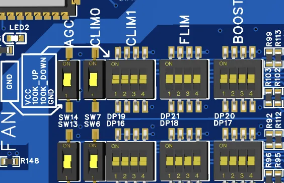
The TB67S249FTG has several pins for configuring AGC parameters — AGC, CLIM0, CLIM1, FLIM, BOOST — and these values are hard to decide before actually running the motors. On top of that, the datasheet says not to change them during operation, so I decided to hard-wire them such that they can’t change even in the presence of a bug, and broke all of these pins out to on-board switches.
AGC and CLIM0 get two positions, high/low, via a 100kΩ pull-up and a slide switch, while CLIM1, FLIM, and BOOST, which take three or more input levels, each get a 4-position DIP switch so you can choose among direct to VCC / 100kΩ pull-up / 100kΩ pull-down / direct to GND. The same arrangement repeats across seven rows, M0 through M6, with column names printed on the silkscreen.
Other driver parameters
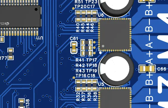
I put 100kΩ on the LTH pin to match the overcurrent latch time to the datasheet’s recommended value, and left the OSCM pin (internal clock configuration) as a jumper array of three 0Ω resistors for selecting VCC or GND.
So after receiving the board you have to remove the seven resistors at positions like R37 and R45 before use. Since the clock is configured with an RC network, not removing the 0Ω jumpers causes a short.
…And a thought while removing those resistors: even if routing got messier, I should have grouped them at the left edge. Being stuck in the middle made it all too easy to disturb neighboring resistors while desoldering — and I did in fact disturb two and had to repair them.
Motor output routing and decoupling
The motor outputs OUTA± and OUTB± are routed as planes, not tracks. The width is about 2.8mm, and plugging that into a calculator gives roughly a 12°C rise at 4.5A. Of course the narrow traces at the IC pins can climb to 80°C, but I arranged things so the heat escapes into the adjoining wide copper and dissipates. Seven terminal blocks are lined up vertically along the right edge of the board to form the motor interface.
For decoupling, each channel has a 100µF electrolytic and a 100nF ceramic right next to the driver — the datasheet’s recommended values. The 100nF path is a touch long, but… it worked fine.
I2C expansion and GPIO expansion
The controller has to handle 8 driver signals per channel — 56 across 7 channels. That’s nowhere near feasible with the available pins on an STM32F446RE (LQFP64), so I routed them by separating timing-critical signals from the rest.
| Signal | Path | Reason |
|---|---|---|
CLK, DIR, EN (x7) | Direct to STM32 (21 pins) | Step pulses must be generated directly by timers, and DIR and CLK must be synchronized |
DMODE0~2 (x7) | 3× MCP23017 (I2C) | Microstep division rarely changes during operation, so I2C latency isn’t a problem |
LO1, LO2 (x7) | 3× MCP23017 (I2C) | Overcurrent/overtemperature latch state is fine to read by polling |
Three MCP23017s provide 48 GPIOs, covering the 35 signals above, and a single I2C bus carries the DAC53608, two TCA9548As, and two TMP112s together. The result: the only pins the controller drives directly are the pulse signals and the DIR that must stay synchronized to them; all remaining configuration and status hangs off one I2C pair.
With eight slaves on one bus, I pre-assigned addresses to avoid collisions.
| Address | Device | Role |
|---|---|---|
0x20~0x22 | MCP23017 x3 | Driver mode/status GPIO expansion |
0x48 | TMP112 #0 | Driver-area temperature |
0x49 | TMP112 #1 | Power-section temperature |
0x4A | DAC53608 | Per-axis current-limit reference voltage |
0x70, 0x71 | TCA9548A x2 | Encoder I2C multiplexers |
So I wouldn’t have to reopen the schematic while assembling or debugging, I printed the address table on the back silkscreen — but once the board was in a case, reading the schematic turned out to be easier anyway. Still, I put it there because I plan to publish this board somewhere like boardrepo, so it wasn’t entirely wasted.
Encoder interface
The magnetic encoders used for joint angle feedback have fixed I2C addresses, so you can’t put several on one bus. So I added two TCA9548A I2C multiplexers, allowing up to 16 channels of identically addressed encoders/sensors.
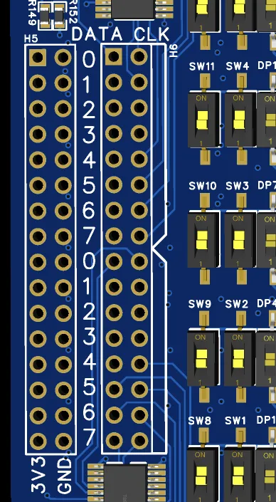
The multiplexers’ downstream channels SC0SC15 and SD0SD15 come out on a 32-pin header, with 3V3 and GND on a separate 32-pin header, and the silkscreen is numbered so each encoder uses four pins (3V3, GND, SDA, SCL). Seven axes only need seven channels, but since I might add a gripper or more sensors later, I broke out all 16.
USB interface
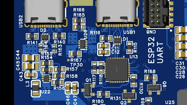
There are two USB ports. USB2 connects directly to the processor’s built-in USB PHY, while USB1 goes through a CP2102N-A02 to the controller’s UART. Both ports have ESD protection via a USBLC6-2P6.
I also added a boot circuit that takes the CP2102N’s DTR and RTS through a pair of MMBT3904 transistors to generate BOOT0 and NRESET, making processor updates convenient.
In short, the USB wired directly to the processor is the external interface that talks to clients and sends commands to the controller, while the USB going through the CP2102N is the ESP32’s debug serial port.
The fun part here was the ESD protection diodes. I’d assumed you use diodes with a high threshold voltage, but it was interesting to learn that in practice you use diodes with a low breakdown voltage.
Thermal management
Thermal failure
When I got the board and first put current through a motor, it spun for about two seconds and stopped. While debugging why on earth that was, I found that over-temperature protection had triggered. I tried adding a heatsink and felt no improvement whatsoever. So I got serious about root-causing it.
The main cause was insufficient thermal vias. On the first order, EasyEDA’s built-in footprint had nine thermal vias by default, so I assumed that was enough and ordered as-is — and then OTP tripped even though the other side wasn’t all that hot.
With a 0.3mm via size and JLCPCB’s 18µm via copper thickness, the copper cross-section per via is
With nine vias, the copper cross-section available for heat to pass through is ≈146,070µm². According to the TB67S128FTG application note, expected dissipation at 3A is ≈9W, so running a 1-D heat conduction calculation with a 1.6mm board thickness and copper conductivity of 401 W/m·K, the temperature difference across the vias is
And at 4.5A, the worst case within rating, dissipation is ≈19W, so
Given the TB67S249FTG’s OTP threshold of 160°C, both cases mean nine vias simply cannot shed that heat at room temperature. So I reordered a new PCB with 57 thermal vias.
…As said above, I really should have just used external FETs.
Adding thermal vias, a heatsink, and fans
Recalculating at 3A with 57 thermal vias:
And assuming the worst case at 4.5A:
Both come out as temperature differences a thermal design can comfortably cover. Counting the heat escaping through the top of the IC and through the FR4, there’s actually even more margin.
Under the drivers I laid thermal vias and spread the heat through GND copper; on the underside I opened the solder mask over those vias, soldered a thin 0.5T copper plate on, and mounted a heatsink on top of that. Air cooling then comes via the fan interface.
Temperature sensing
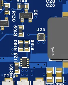
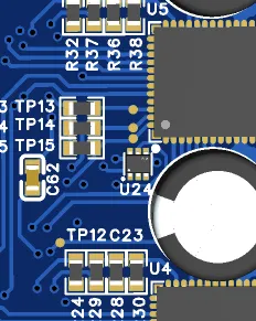
The temperature sensors are two TMP112Ds (U24, U25). They attach to the controller over I2C and are polled each cycle to refresh their state. One sits on the right side of the board where driver heat concentrates and the other on the left where the power section is, so localized heating and overall board temperature can be told apart.
As I’ll mention later, it would have been better to attach the temperature sensors to the processor instead.
Fan interface
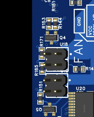
There are two fan channels, each connector carrying four pins: 12V, GND, PWM, and tach sense. PWM is open-drain driven by an MMBT3904 so it can drive a 12V fan’s control input directly, and the sense line is pulled up and fed to the processor’s input capture so actual RPM can be read.
It connects to the processor and uses the MCPWM peripheral. RPM is computed using the MCPWM timer’s capture.
What I regret
Things I learned only after building the board and actually running it.
- The temperature-fan control loop spans two chips.
The TMP112 sits on the I2C bus the controller reads, while fan PWM and sense hang off the processor. So even spinning a fan requires a round of inter-chip communication. It would have been cleaner to put temperature sensing on the same processor as the fans. Moreover, it’s better for the driver side to handle driving only — temperature measurement can bottleneck timer parameter updates while the drivers are running.
- Heat dissipation was impossible.
As described above, the thermal vias were nowhere near enough. The main cause was keeping the default footprint after reading only the datasheet — never the application note — and therefore knowing only how to use the part. Honestly, I still wonder why the datasheet omitted thermal parameters, and why EasyEDA’s default footprint had to come with nine vias pre-placed, of all things, leaving me with no reason to even suspect the thermal vias. Still, the experience gave me the habit of reading other documents carefully.
- Encoder input latency is severe.
In the current design, actual joint angles come from I2C magnetic encoders, which hurts real-time performance. But reading A/B phases all at once instead would need seven more timers, which would have meant something like adding another MCU.
An architecture I’d like to try next time
Fixing the regrets above goes without saying; next time I’d also like to try an architecture with one MCU like an STM32F103 per motor. The idea is to let each axis handle encoder input and pulse generation on its own.
- Provide a common clock source and run in HSE bypass mode to synchronize clocks (obviously the clock structure must be identical across the slave MCUs)
- Each slave MCU receives a command for how many steps to turn the stepper over a given time. These commands can queue up.
- Each slave MCU gets pins for encoder input and for synchronizing the measurement instant.
I’d like to build, at some point, an architecture where encoder reads and timer parameter adjustments can happen perfectly simultaneously.
Datasheet references